
In the highly competitive and rapidly evolving landscape of semiconductor manufacturing, one often overlooked yet crucial aspect is the role of low outgassing plastics. These materials are vital in maintaining the integrity of high vacuum environments and preventing contamination risks that could compromise product quality and performance. Join us as we delve into the fascinating world of outgassing for semiconductor plastics, uncovering their importance, the right materials for the job, and the techniques to minimize outgassing in semiconductor applications.
Key Takeaways
- Low outgassing is essential for semiconductor manufacturing to prevent contamination and mitigate potential risks.
- Materials used in semiconductors must have chemical/abrasion resistance, heat resistance, and low outgassing rates. Fluoropolymers & high performance plastics such as PEEK & PFA are commonly used due to their properties.
- Various techniques such as material selection/handling, surface cleaning/treatment, baking/temperature control can help minimize outgassing in semiconductor applications. Atlas Fibre provides expert machining services for these materials.
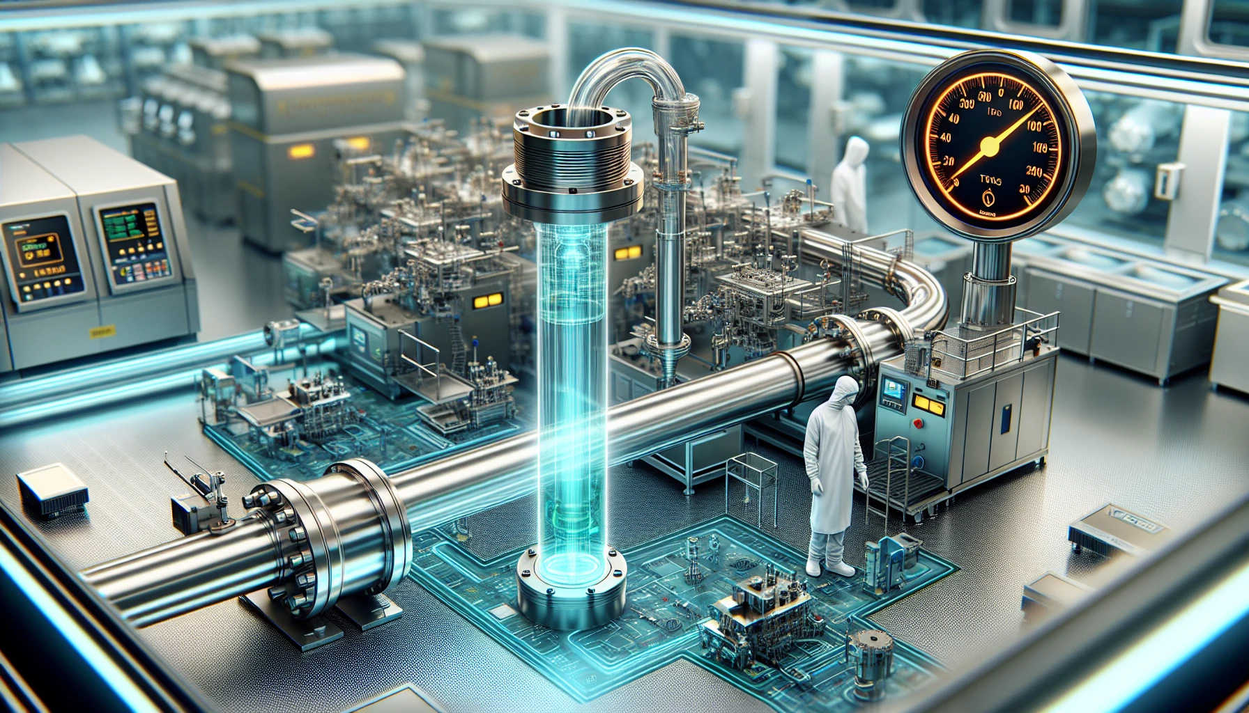
The Importance of Low Outgassing in Semiconductor Manufacturing

Outgassing is the emission of gases and vapors from surfaces when placed in a vacuum environment. In semiconductor manufacturing, the emphasis on low outgassing arises from the need for high vacuum environments and the prevention of contamination that could negatively affect the product’s quality and efficiency. Most plastics tend to have a high outgassing rate, which is problematic for the semiconductor industry as it requires strict adherence to outgassing standards.
The risks associated with plastic outgassing are not limited to the manufacturing process. Contact with volatile organic compounds (VOCs) can cause:
- Irritation of the eyes, nose, and throat
- Coughing
- Headaches
- Dizziness
- Nausea
High purity plastics can help minimize these risks, making material selection a critical aspect of the production process.
High Vacuum Environments
Thin film deposition benefits greatly from high vacuum environments, which enhance the mean free path of particles moving from the target to the substrate. This decreases the presence of unwanted particles in the chamber, resulting in:
- more uniform and pure thin films, even under high temperatures
- reduced impurities in semiconductor manufacturing equipment
- regulated chemical reactions
- increased accuracy in processes such as etching, depositing, and cleaning wafers
Vacuum technology is employed in semiconductor manufacturing equipment to guarantee optimal performance and quality.
The upkeep of a high vacuum environment within a semiconductor manufacturing setting necessitates:
- the reduction of contamination
- control of energy costs
- precision in deposition and etching processes
- the maintenance of cleanliness and controlled conditions
Additionally, the high cost and complexity of vacuum chamber equipment may also present challenges. To overcome these challenges, materials with low outgassing rates are employed to reduce contamination and preserve the integrity of the vacuum environment.
Contamination Risks
Outgassing has the potential to damage equipment and negatively impact product quality within semiconductor manufacturing. The primary sources of outgassing are surfaces of any material that adsorb gases and vapors and release them when placed in a vacuum. Outgassing can result in contamination of the vacuum chamber and harm to the manufacturing environment.
Outgassing can have extensive implications on the quality of semiconductor products. It can introduce extra gases and condensable materials into the wafer environment, leading to defects, yield loss, and contamination events. To mitigate these risks, choosing materials that are good electrical insulators is crucial.
Selecting the Right Plastic Materials for Semiconductors
The selection of appropriate plastic materials for semiconductors requires consideration of factors like high temperature resistance and chemical and abrasion resistance, which contribute to the durability and lifespan of the semiconductor components. High-performance plastics such as Fluorinated Ethylene Propylene (FEP), Polyether Ether Ketone (PEEK), and Polytetrafluoroethylene (PTFE) are commonly employed for their outstanding heat resistance properties in the semiconductor industry.
High Temperature Resistance
High temperature resistance is a critical factor in the selection of plastic materials for semiconductors. Plastics with high temperature resistance can endure the extreme temperatures encountered in semiconductor manufacturing processes without warping or deteriorating. For instance, temperatures may reach up to 1200°C for certain thermal processes.
High-performance thermoplastics such as:
- Vespel
- FEP
- PEEK
- PTFE
are commonly employed for their outstanding heat resistance properties in the semiconductor industry.
High temperature can notably accelerate the outgassing rate in plastics, leading to problems such as blistering, delamination, and emission of gases and hydrocarbons. As a result, it is crucial to select materials with high temperature resistance to minimize the effect of high temperatures on outgassing rates.
Chemical and Abrasion Resistance
When choosing plastic materials for semiconductors, chemical and abrasion resistance are vital as the materials must withstand the chemicals used in manufacturing and resist wear during handling and assembly. Chemical resistance refers to the plastic’s capacity to withstand contact with various chemicals without suffering degradation or harm. Abrasion resistance is essential for plastics used in semiconductor production to ensure the production of a quality product that is free from defects. It helps to reduce wear, erosion, and particulate contamination in the semiconductor manufacturing process.
Chemical and abrasive materials can have an effect on plastics used in semiconductor manufacturing by examining their chemical resistance and inducing physical changes through abrasion and material removal. The BS EN ISO 5470 Abrasion Resistance Test and the BS ISO 4649 Abrasion Resistance Test are utilized to evaluate the chemical and abrasion resistance of plastic materials.
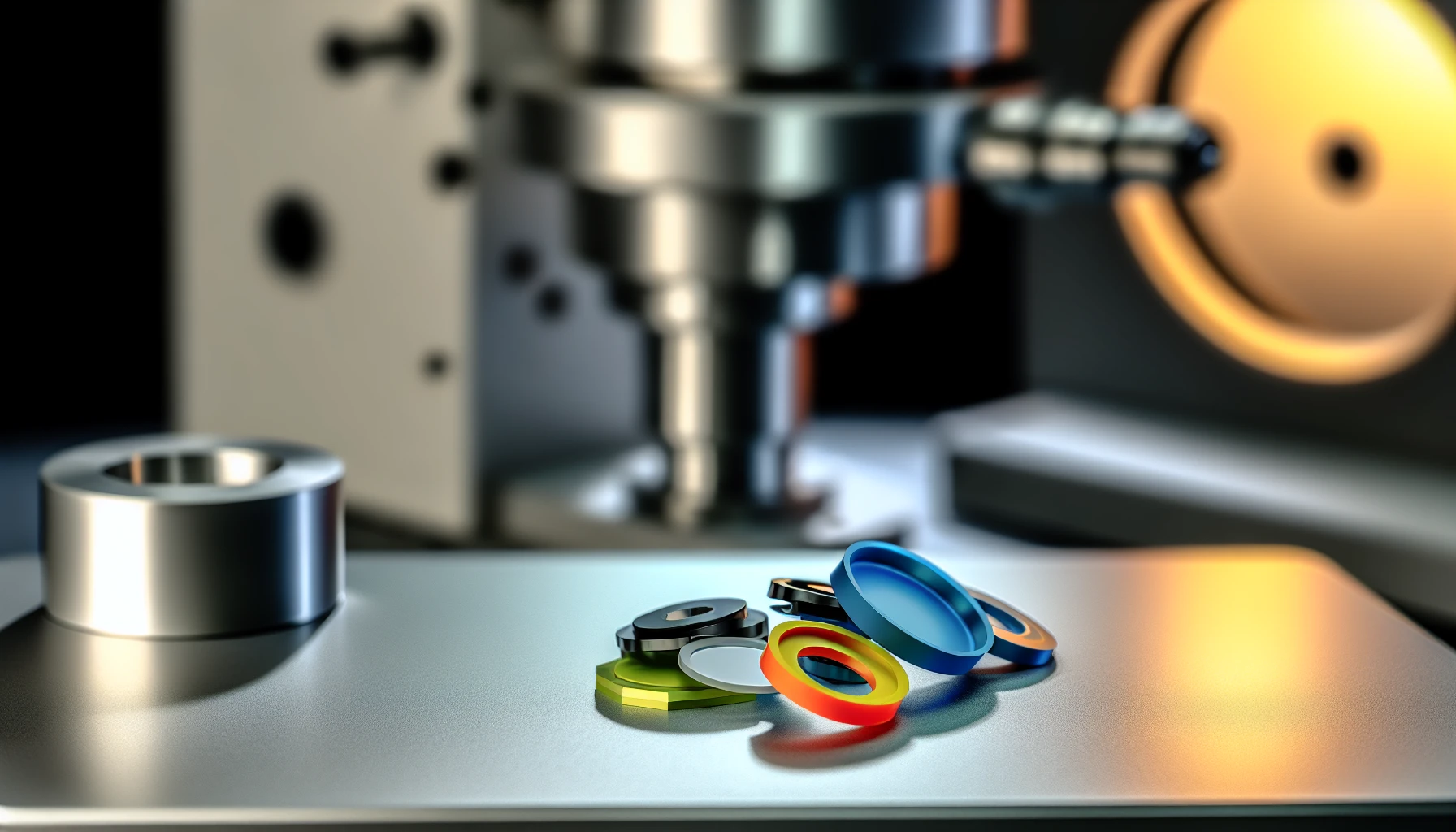
Common Low Outgassing Plastics Used in Semiconductor Manufacturing
Low outgassing plastics frequently used in semiconductor manufacturing encompass fluoropolymers and high-performance plastics such as PEEK and PFA. These materials offer low contamination and high-performance properties, making them ideal choices for semiconductor applications.
Subsequent sections will delve deeper into these types of plastic components and their application on plastic surfaces.
Fluoropolymers
Fluoropolymers are a popular choice for low outgassing applications due to their excellent chemical resistance and low contamination properties. Polytetrafluoroethylene (PTFE), Fluorinated Ethylene Propylene (FEP), and Perfluoroalkoxy (PFA) are the fluoropolymers employed in semiconductor manufacturing. The essential characteristics of fluoropolymers include chemical resistance, electrical resistance, high temperature resistance, non-stick properties, and non-toxicity.
Fluoropolymers contribute to purity and offer superior chemical resistance in semiconductor production. They offer a high degree of chemical resistance to a broad range of chemicals, such as acids, bases, and organic solvents. Fluoropolymers are indispensable for preserving the quality and integrity of semiconductor fabrication processes and are employed in pipes, vessels, valves, and pumps within semiconductor fabrication facilities.
High-Performance Plastics
High-performance plastics like PEEK and PFA are also apt for low outgassing applications in semiconductor manufacturing. These plastics offer low-outgas properties, making them ideal for use in vacuum systems and high-purity applications in the semiconductor industry. PEEK has a temperature resistance of up to 250°C (482°F), while PFA exhibits a high temperature tolerance of 260°C (500°F).
The characteristics of high-performance plastics in the context of semiconductor manufacturing include:
- Outstanding chemical resistance and abrasion
- Ability to withstand harsh conditions
- Maintaining shape and integrity in manufacturing processes
- Low outgassing rates
- Exceptional mechanical properties
These materials play a vital role in ensuring the quality and reliability of semiconductor devices.
Techniques to Minimize Outgassing in Semiconductor Applications
To mitigate outgassing in semiconductor applications, a range of techniques such as apt material selection and handling, surface cleaning and treatment, and baking and temperature control can be utilized.
These techniques will be examined in detail in the subsequent sections.
Material Selection and Handling
Material selection and handling involve choosing suitable low outgassing materials and guaranteeing their correct storage and handling to minimize contamination. Factors to consider when selecting low outgassing materials for semiconductor applications include:
- Total Mass Loss (TML)
- Collected Volatile Condensable Materials (CVCM)
- Water Vapor Regain (WVR)
- The specific function of the material
- Its purity
- Its outgassing characteristic
PEEK, PPS, Delrin (POM), Teflon (PTFE), non-anodized aluminum, and electroless nickel are the most effective materials for limiting outgassing in semiconductor manufacturing.
Material handling plays a significant role in reducing outgassing in semiconductors. Contaminants like dust, oils, and residues from handling may be introduced, leading to outgassing when the semiconductors are exposed to high temperatures or vacuum conditions. Furthermore, physical damage like scratches or cracks can create pathways for outgassing. As such, it is essential to use proper handling techniques and maintain clean environments to minimize outgassing in semiconductors.
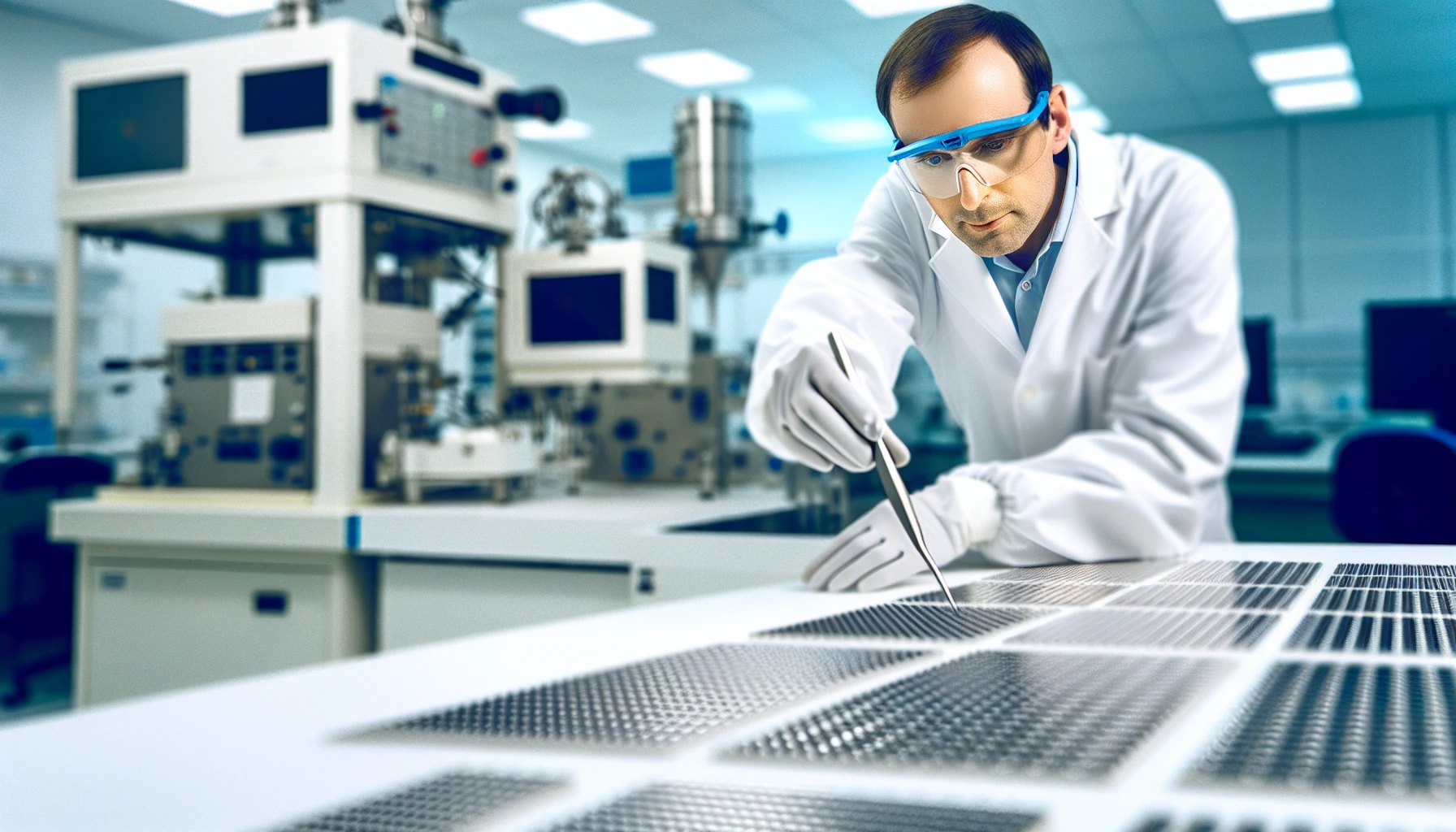
Surface Cleaning and Treatment
Surface cleaning and treatment play a crucial role in semiconductor manufacturing for reasons such as contaminant removal, contamination prevention, adhesion enhancement, electrical properties improvement, and uniformity assurance. Surface cleaning techniques that may prove beneficial in limiting outgassing in semiconductor applications include cleaning and handling (bakeout), surface treatment, passivation, wet wafer cleaning methods, utilization of cleaning solutions such as piranha cleans and isopropyl alcohol, and UV/ozone cleaning methods.
Surface treatment, such as coating treatments, can reduce outgassing rates in semiconductor manufacturing. Applying coatings to the surfaces of vacuum systems can help minimize the emission of gases from the treated surfaces, thus diminishing the potential for contamination in the semiconductor manufacturing process. Selecting materials with low outgassing rates and implementing vacuum pre-bake can help to reduce the effects of outgassing in semiconductor manufacturing.
Baking and Temperature Control
Baking represents a critical step in reducing outgassing in semiconductor production. It aids in the removal of volatile molecules from circuit board materials. Here’s how it works:
- Heating the materials to a high temperature, typically between 100 to 125°C.
- This accelerates the outgassing process and eliminates impurities.
- Decreases the chances of outgassing during semiconductor production.
Temperature control plays an integral role in mitigating outgassing during semiconductor manufacturing by minimizing the release of volatile organic compounds (VOCs) from materials and components. By maintaining a controlled temperature environment, the outgassing rate is reduced, thereby helping to prevent contamination and preserve the purity of the semiconductor manufacturing process.
Additionally, temperature control can also help to enhance the performance and reliability of semiconductor devices.
Case Study: NASA’s Approach to Low Outgassing Materials

NASA’s strategy regarding low outgassing materials underscores the significance of material selection and testing to ensure adherence to stringent outgassing requirements. As per NASA standards, a material is considered low-outgassing if its Total Mass Loss (TML) is less than 1%, and its Collected Volatile Condensable Materials (CVCM) is less than 0.1%. NASA’s process for testing for low outgassing materials involves placing the materials in a test chamber and removing the air to simulate the vacuum of space, using the ASTM E595 test method to establish the outgassing requirements.
NASA’s emphasis on low-outgassing materials has had an impact on a number of projects and missions. For instance, 3D Printing has been enabled by certain materials that meet NASA’s standards for low outgassing. Additionally, the Outgassing Lab at Goddard Space Flight Center has tested and validated various varieties of Parylene, which are ultrathin coatings that protect spacecraft from outgassing.
Furthermore, NASA has developed tests to screen materials for low outgassing, which is essential for selecting materials for space applications. These examples demonstrate the crucial role of low outgassing materials in maintaining the integrity and performance of space missions and projects.
Industry Standards and Compliance
Compliance with industry standards, such as ASTM E595, aids in ensuring that materials used in semiconductor manufacturing satisfy low outgassing requirements and uphold product quality. This standard includes two primary characteristics: total mass loss (TML) and collected volatile condensable matter (CVCM). By adhering to these standards and implementing rigorous quality control measures, manufacturers can reduce the risk of outgassing and contamination in their products and processes.
In addition to ASTM E595, ISO class 7 or ISO class 8 cleanrooms are industry standards that must be met to control outgassing and other sources of contamination in semiconductor cleanroom environments. Adherence to these standards and others helps to promote innovation, cost-effectiveness, and the development of comprehensive solutions in the semiconductor industry. Furthermore, standards guarantee that semiconductor devices and integrated circuits meet the necessary specifications and quality criteria, ensuring product excellence.
Choosing the Right Machining Partner for Low-Outgassing Plastics
The selection of an appropriate machining partner for low-outgassing plastics requires consideration of the following factors:
- Standards compliance
- Capabilities
- Experience
- Quality control procedures
- Material selection expertise
- Communication
The following sections will address the significance of expertise in machining low-outgassing plastics, the use of appropriate coolants, and the establishment of suitable quality management systems.
Atlas Fibre is an Expert at Machining High Performance Low-Outgassing Plastics
Atlas Fibre possesses significant experience in machining low-outgassing plastics, providing precision fabrication and machining services for engineering thermoplastics. They are proficient in surface treatments like machining and electropolishing, which produce smooth surfaces that minimize adsorption sites. With over six decades in the industry, Atlas Fibre is uniquely qualified to machine low-outgassing materials and ensure high-quality results.
Atlas Fibre offers the following services:
- Maintains a large stock of thermoset materials
- Offers same-day shipping for orders placed before 1:00 PM CT
- Conducts batch and sheet testing to ensure quality control and assess the properties of the plastics
- Provides extensive expertise and experience in machining thermosets
With these services, Atlas Fibre is an ideal partner for machining low-outgassing plastics.
Using the right coolants
The use of suitable coolants is crucial to minimize outgassing during machining processes. Non-aromatic, water-soluble coolants and air-based coolants are the most suitable coolants for machining low-outgassing plastics. High-performance materials such as Torlon PAI and Celazole PBI may require the use of coolants, while Nylons, being hygroscopic, may be better machined with spray mist or air instead of coolant.
Selecting the right coolant not only reduces the risk of outgassing but also ensures the longevity and performance of the materials being used. By making an informed choice of coolant, one can reduce the outgassing effect and maintain a clean and controlled environment during the machining process.
Having the right quality management systems
The implementation of appropriate quality management systems guarantees the fulfilment and maintenance of low outgassing requirements throughout the manufacturing process. These systems guarantee that all materials used in semiconductor manufacturing are sourced to be non-particle shedding and non-outgassing. Furthermore, quality management systems feature processes for testing and monitoring outgassing levels to identify any potential issues and take corrective actions.
A quality management system for low-outgassing plastics machining should encompass the following:
- Material selection
- Supplier qualification
- Incoming material inspection
- Machining process control
- Quality assurance
- Documentation and traceability
- Continuous improvement
By adhering to these guidelines and implementing rigorous quality control measures, manufacturers can ensure the quality and reliability of their products.
Summary
In conclusion, low outgassing plastics play a critical role in ensuring the quality and reliability of semiconductor manufacturing processes. By selecting the right materials, adhering to industry standards, and employing the appropriate techniques, manufacturers can minimize outgassing and contamination risks. Furthermore, partnering with experienced machining companies like Atlas Fibre can guarantee a smooth and efficient production process. As the demand for high-performance semiconductors continues to grow, the importance of low outgassing plastics will only become more paramount in maintaining the integrity and performance of these essential devices.
Frequently Asked Questions
What is outgassing, and why is it important in semiconductor manufacturing?
Outgassing is the emission of gases and vapors from surfaces in a vacuum environment, which is crucial for maintaining high vacuum environments and avoiding contamination issues in semiconductor manufacturing that could impact product quality and efficiency.
What types of plastics are commonly used in semiconductor manufacturing for low outgassing applications?
Common plastics used for low outgassing applications in semiconductor manufacturing are fluoropolymers like PTFE, FEP and PFA, as well as high-performance plastics like PEEK and PFA.
What techniques can be used to minimize outgassing in semiconductor applications?
To minimize outgassing in semiconductor applications, proper material selection and handling, surface cleaning and treatment, as well as baking and temperature control are recommended techniques.
What is the ASTM E595 standard, and how does it relate to low outgassing materials?
ASTM E595 is a standard used to assess the outgassing performance of materials, which includes two primary characteristics: total mass loss (TML) and collected volatile condensable matter (CVCM). Compliance with this standard helps ensure that low outgassing requirements are met for materials used in semiconductor manufacturing.
How does NASA approach low outgassing materials for space applications?
NASA adopts a rigorous approach to selecting and testing materials to ensure they are suitable for low outgassing space applications. They use the ASTM E595 test method and have developed their own proprietary materials to meet these requirements.